With the growth in wearables and more recently in micro-sized wearables, one of the key challenges is how to fit all the required functionality onto extremely small circuit boards used. Smartwatches may have more functionality packed into them, but relatively speaking there is plenty of space when you consider an earbud or even smart jewellery. For highly efficient on/off switching, designers now have the option of a tiny (0.63 x 0.33 x 0.25 mm) small-signal MOSFET to save vital board space and battery power.
They say size matters, and when it comes to wearables and smart jewellery that is clearly true. Just take a look at the PCB space available on a pair of wireless earbuds. And while most of the functionality comes from embedded software features, there is still a lot of hardware that needs to be integrated into the final design: from the microphone and speaker through to RF components for Bluetooth communications. That means there is even greater pressure on essential functionality to take up the smallest footprint possible.

Every 0.1 millimeter counts
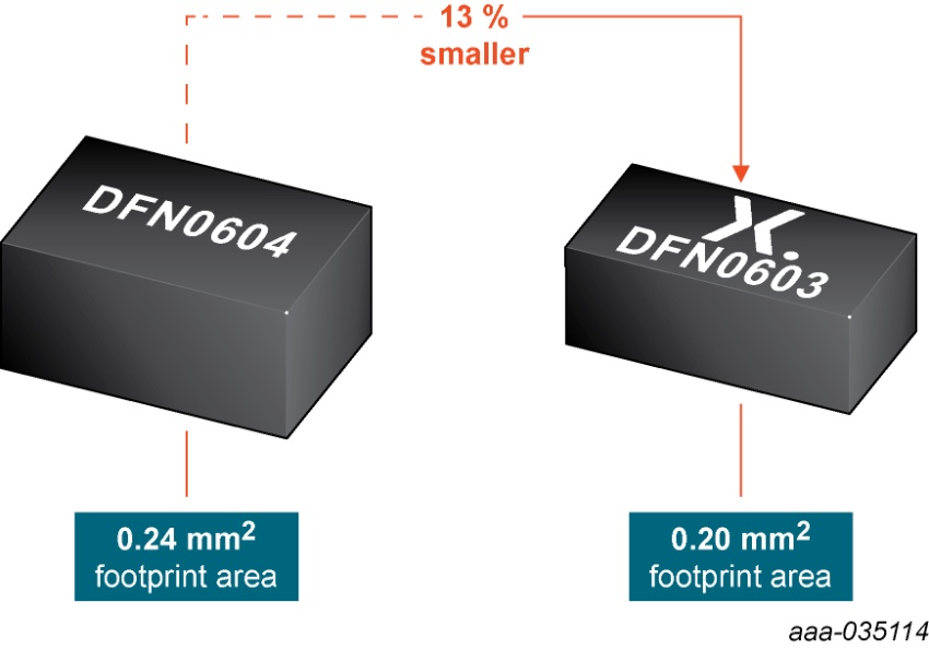
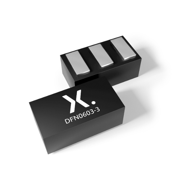
For example, there are a number of options when it comes to handling simple on/off switching. But many designers using a MOSFET to do this have only been able to go as small as 0.6 x 0.4 mm (DFN0604). With Nexperia releasing a new range of small-signal MOSFETs in a proven DFN0603 package (0.63 x 0.33 x 0.25 mm), designers can now save an additional 13% of board space alongside a significant height reduction. Providing the optimum flexibility of choice to engineers with the challenge of increasing functionality and performance of systems, whilst reducing PCB size.
An extremely efficient option
While size is critical, in many respects the real benefit of Nexperia’s DFN0603 MOSFETs is their RDSon. Options are available rated at VGS of 4.5 V with a typical RDSon as low as 122 mΩ. In some cases that is a reduction of approximately 74% compared to commercially available DFN0604 products. Such a significant reduction in RDSon naturally brings many benefits in terms of efficient switching even at higher switching frequencies.
Given Nexperia’s clear understanding and leadership in the development of tiny packages, using the proven DFN0603 package for small signal MOSFETs was an obvious step forward. In addition to providing excellent thermal conduction, Nexperia has also been able to embed electrostatic discharge (ESD) protection into some members of the family, providing additional flexibility with this tiny solution.

A growing portfolio
The first devices from the new range include four products which have been released to production and two additional products that are scheduled to be released shortly. Nexperia is continuing to development the range of ultra-small MOSFETs, helping deliver further options for space-constrained designers regardless of their application.