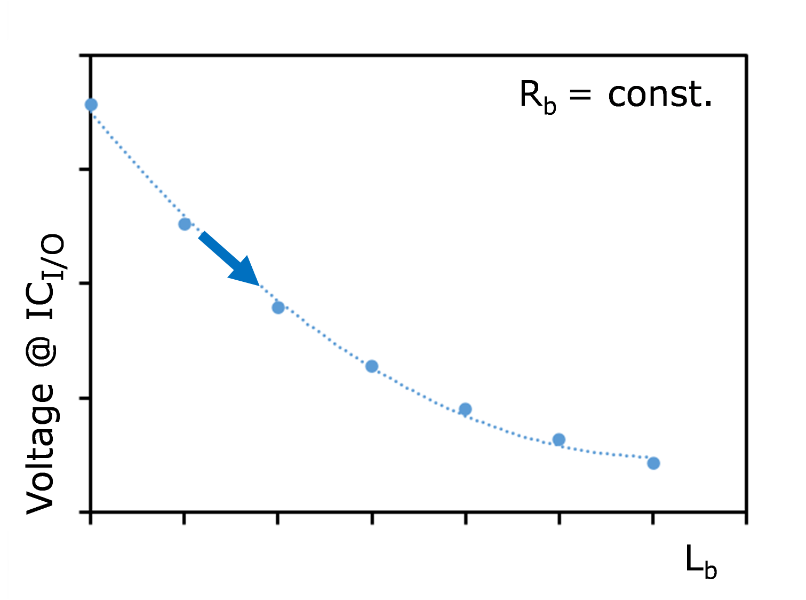
To utilize the full data rate of USB4™ (or Thunderbolt™ 4), it is popular to use retimer or redriver devices on superspeed data lines. This has consequences on the ESD protection approach, which may not be completely obvious. Typical USB3.2 systems can have trace lengths exceeding 100 mm. The placement of a retimer or redriver device will result in a significantly shorter trace length with a subsequent positive impact on signal trace inductance. As a rule-of-thumb, a 10 mm trace length equates to roughly 3-3.5 nH of inductance. While a reduction of the trace inductance is certainly desirable from the view of signal integrity, a reduction of the inductance between ESD protection and the protected system will also increase the peak voltage seen by the protected system.

ESD failure mechanisms and trace length
There are two main ESD failure mechanisms for the protected IC. One is a thermal failure caused by the residual current flowing into the IC. In the quasi-static case, this current is dependent on the ratio of the on-state resistance ratio of the path into the IC and the path to ground via the ESD protection.
The second ESD failure mechanism is exceeding the maximum electric field strength over the gate oxide in the transceiver of the protected system. To reduce the electric field strength, the peak clamping voltage seen by the protected chip should be minimized. This dynamic effect cannot be captured by quasi-static considerations. Decreasing the signal trace length reduces the board inductance Lb between external ESD protection and protected chip. For an otherwise unchanged system, this will increase the hazardous ESD peak voltage.
Determining peak suppression performance
To counter this effect, Nexperia has just released the first products in the latest TrEOS technology which are optimized for peak voltage reduction. But how can you discover which protection device is suitable to protect which system? To support design engineers in choosing the right protection device for their system, Nexperia is offering fully-dynamic System Efficient ESD Design (SEED) simulation models for their high-speed ESD devices. Contrary to quasi-static models, fully dynamic SEED models allow the system-level simulation of the peak voltage suppression as well.

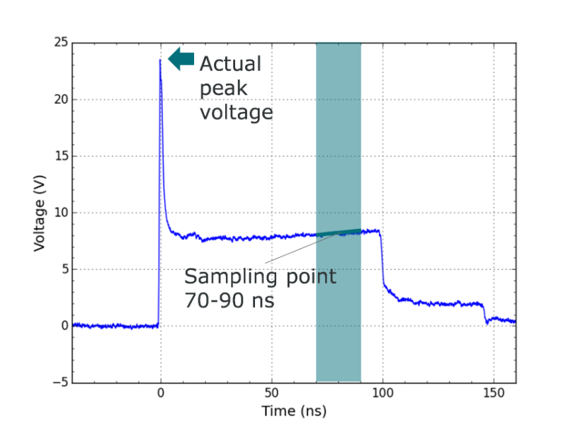
Determining the peak suppression performance of an ESD protection device is less straightforward than one might expect. ESD guns are designed to test the robustness of complete systems but lack the accuracy to show the peak voltage in sensitive transceiver systems. Variations can be significant, even between two measurements in an unchanged system. Transmission-Line Pulse (TLP) measurements can show a significantly higher reproducibility compared to ESD gun measurements. However, data sheets typically show only the standard TLP I(V) curve sampled when the protection device has switched on. The 100 ns pulse length is chosen to evaluate the thermal failure mode of an IEC61000-4-2 ESD pulse.
To evaluate the peak voltage, a very fast TLP (vfTLP) measurement is done. This is the most accurate measurement of the short overvoltage occurring at the beginning of the pulse, enabling investigations above the transient triggering effect during the first nanoseconds.
Re-timer in action
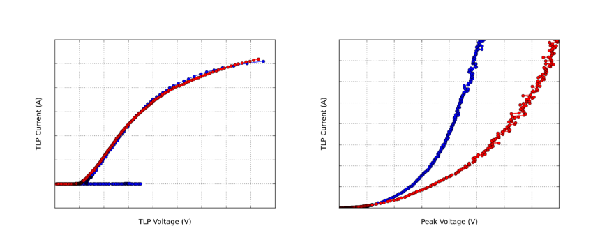
To give a practical example, we compared the clamping of two ESD protection devices with comparable capacitance. While both devices are comparable in standard TLP clamping voltage, thus energy suppression of the second peak of an ESD pulse, we would intuitively assume that the red device would have a better peak voltage suppression compared to the blue device However, this is not the case if we plot the actual vfTLP peak voltages versus vfTLP currents. The rise time has been chosen to be 600 ps to represent the first fast peak of an IEC61000-4-2 pulse.

In the first scenario despite a higher TLP trigger voltage Vt1 of the blue curve the same device offers a lower vfTLP peak voltage over the protection range, which results in a lower peak voltage at the IC. As an additional benefit, the blue device’s higher reverse standoff voltage VRWM allows placement directly behind the connector in an USB Type-C® environment. This comes with the advantage of adding more inductance between protection and IC, further reducing peak voltages. In the white paper Choosing ESD protection devices for USB4 we discuss that USB Type-C can connect USB3.2 systems with their higher voltage specification limits to USB4 systems. So protection devices for USB4 should be backwards compatible to USB3.2 regarding VRWM when placed right behind the connector. In this position it also provides protection for the AC coupling capacitance.
Delivering practical solutions
Using retimer or redriver devices in USB4 environments will shorten signal traces between ESD protection and protected IC, resulting in lower board trace inductances Lb. While shorter traces are certainly beneficial for signal integrity, their lower inductances will increase peak ESD voltages when comparing otherwise unchanged systems. To counter this effect, Nexperia can offer devices in the latest TrEOS technology which are optimized for peak voltage suppression.
Would you like to learn more about SEED or ESD protection in general? Please refer to our ESD Design Engineer's Guide.