The increasing number of electronic functions in modern cars must be realized within a given space. This space limitation has led to a growing device density on printed circuit boards (PCBs), necessitating components to shrink in size. However, smaller packages need to dissipate the same amount of heat on a reduced footprint, leading to a higher power density on the board. DFN packages with their compact dimensions and thermal properties are the right choice to replace bulky leaded packages on PCBs.

For decades leaded SMD packages have been the industry standard for discrete electronic devices. The structure of perhaps the most prominent package is the SOT23, where the die is positioned on a leadframe which together with the metal pads is fully encapsulated.
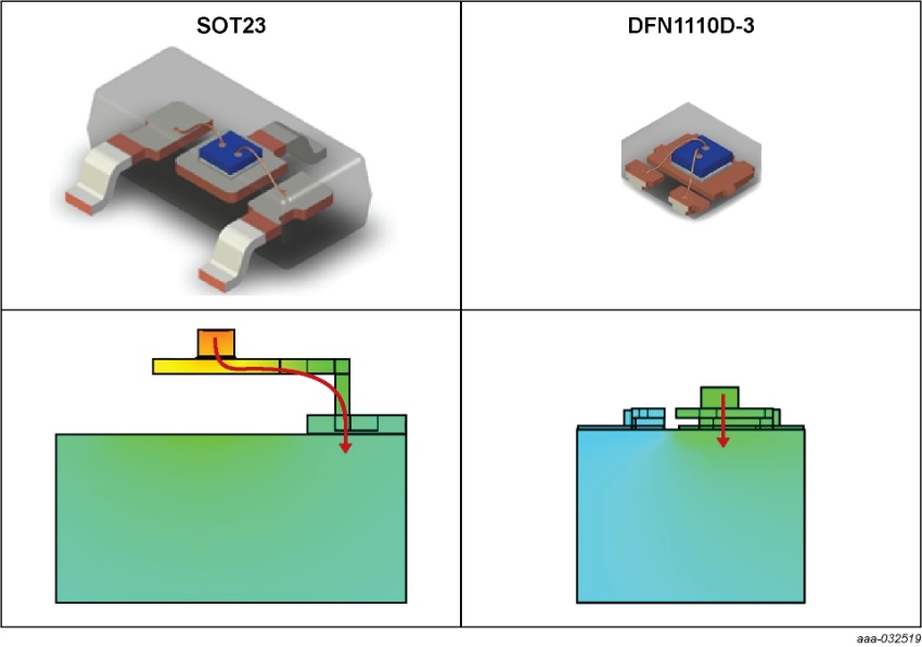
This means heat conduction is the dominant heat transfer mechanism, as heat convection and radiation are almost irrelevant in the given structure and temperature range. The generated heat is conducted through the die attach layer into the leadframe, and from there it flows through the long leads into the PCB. Figure 1 shows a cross-section of a SOT23 packaged device along the leadframe and across the middle of the package – highlighting the heat path.
Straight to the board
With the DFN1110D-3, Nexperia’s DFN counterpart of SOT23, there are no external leads. With no leads and shorter bond wire lengths, DFN packages have less parasitic inductance compared to their leaded counterparts. The metal pads are also more compact and closer to the leadframe. In this way, the package dimensions reduce significantly while still having the same leadframe size below the die. The leadframe effectively serves as an exposed heatsink and electrical contact at the bottom of the package, allowing the heat to flow directly from the die into the PCB.
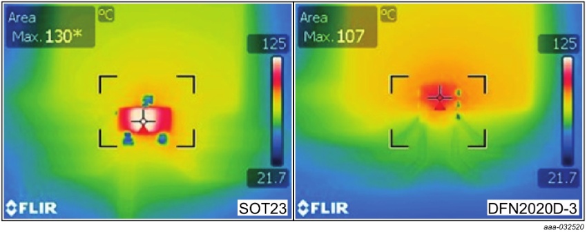
Despite the DFN package’s very compact dimensions, it has an excellent power dissipation capability. However, using a PCB with low thermal resistance and sufficient thermal conductivity is mandatory to allow for proper lateral heat spread. The infrared pictures in Figure 2 illustrate the high-power density, showing a comparison between a SOT23 and DFN2020D-3 dissipating the same power (250 mW). The higher power density and good dissipation of the DFN2020D-3 are evident, especially as there are no white spots on the package.

DFN1110D-3 versus SOT23
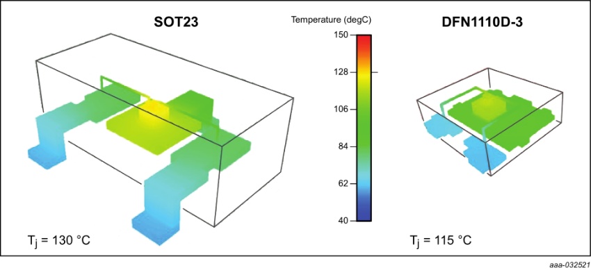
In simulation tests, using a standard FR4 PCB with 35 μm thick copper (Cu) lanes and an ambient temperature of 25 °C, a dissipated power of 250 mW is assumed, which leads to a junction temperature of 130 °C for the SOT23 and 115 °C for the DFN1110D-3. The lower junction temperature of the die in the DFN package for a given dissipated power level can also be used as extra headroom if de-rating the maximum junction temperature is required due to reliability standards for a specific application. Here, the device runs much cooler while delivering significant space savings on the PCB.

The solution for excellent thermal conduction
Automotive-qualified DFN packages with their compact dimensions are the right choice for replacing bulky leaded packages on PCBs. The higher power density that arises from densely populated PCBs requires packages with excellent thermal capability. Thanks to their exposed heat sink and optimized heat path, DFN packages satisfy this requirement. However, to take full advantage of DFN packages, PCB types with improved thermal conductivity are recommended.
For further details please read our application note AN90023 Thermal performance of DFN packages.