Automotive electronics are evolving faster than ever. Traditional internal combustion engine (ICE) architectures are giving way to mild hybrids, plug-in hybrids and fully electric vehicle (EV) platforms. At the same time, infotainment systems and body electronics are becoming more sophisticated and feature-rich, with car manufacturers consolidating multiple functions under zonal controllers rather than relying on an ever increasing number of distributed control units. These shifts are redefining not just the role of components such as automotive MOSFETs, but critically how they are packaged to balance performance, reliability and cost. Nexperia’s MLPAK family was developed with these trends in mind, delivering compact, scalable, reliable MOSFETs optimized for modern automotive subsystems like body control, lighting and infotainment.
From ICE to EV: changing demands for power MOSFETs
Traditional ICE platforms employed 12 V systems to power auxiliary loads, and the electronics (often located near the engine) were exposed to under-the-hood temperatures as high as 125 °C. By contrast, electric vehicles typically operate at 48 V or more, but maximum operating temperatures rarely exceed 85 °C. This shift lowers thermal extremes but increases current densities, making conduction losses and switching performance more critical than ever.
Industry recognized automotive leaded packages were designed to cope with harsh thermal and environmental conditions. However, they are increasingly viewed as overkill for non-safety critical applications in modern EV subsystems. Alternatively, while fully leadless packages offer board space savings and ease of assembly they can suffer solder-joint degradation under repeated thermal cycles. The industry clearly needed a middle ground: a scalable packaging solution that is compact, robust and reliable for high-volume production.
MLPAK: bridging the gap
Nexperia’s MLPAK family was developed to meet this exact need. It combines the compact efficiency of micro-lead packages with the mechanical strength of traditional leaded designs – an ideal balance for next-generation automotive applications.
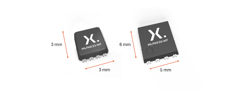
- MLPAK33-WF (3×3 mm): optimized for space-constrained designs
- MLPAK56-WF (5×6 mm): designed for higher-current or thermally demanding loads

Maintaining more than 80% solder coverage after harsh thermal cycling, MLPAK delivers robust mechanical integrity. Devices are AEC-Q101 qualified and feature side wettable flanks, enabling automated optical inspection (AOI) and reducing the need for costly X-ray inspection – essential for today’s high-volume automotive manufacturing.
Tailored technology for modern applications
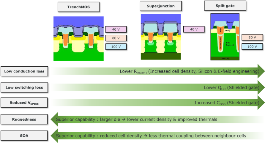
MLPAK isn’t just a package, it’s part of a broader strategy that aligns silicon technology with application-specific needs. By offering differing MOS innovations like trench, split-gate and superjunction, Nexperia ensures designers can choose the right balance of ruggedness, efficiency, and scalability.
- 40 V technology - rugged, strong SOA / avalanche capability, suited for motor controls like seat adjustment and wipers
- 60 V technology - balances ruggedness and switching efficiency, ideal for 48 V auxiliary DC-DC converters and lighting systems
- 80 / 100 V technology - optimized for high switching efficiency, perfect for high-efficiency 48 V lighting, main beam headlights and boost DC-DC converters
This architecture minimizes gate charge, reduces conduction and switching losses, and ensures robust electrical, thermal and mechanical performance across automotive applications. Additional benefits include reduced EMI, smaller system size and footprint compatibility with LFPAK, allowing designers to reuse existing layouts without compromise.

Future-proof packaging for modern vehicles
Automotive electrification is evolving rapidly and scalable MOSFET packaging is vital. Nexperia offers a future-proof solution with MLPAK, that combines the compactness of leadless designs with the mechanical resilience of leaded packages. Available in 40 V, 60 V, 80 V and 100 V variants, AEC-Q101 MLPAK devices deliver high efficiency, reliability, footprint compatibility and scalable deployment across multiple applications. From lighting to motor drives to DC-DC converters, MLPAK offers designers a flexible platform capable of meeting the evolving nature of next-generation high-volume automotive electronics.
Explore the full MLPAK33-WF and MLPAK56-WF automotive MOSFET range to learn how scalable, high-volume automotive MOSFET packaging can accelerate your next design.