Compared to MOSFETs, drawbacks of conventional bipolar junction transistors (BJT) included their requirement for a continuous base current and relatively higher saturation voltage across their collector-emitter terminals. These have the effect of increasing power dissipation, making them unsuitable for use in applications like load switches and LDOs. This blog article shows how the high current gain (hFE) and very low saturation voltage (VCEsat) of Nexperia’s high-performance ‘low VCEsat‘ BJTs reduce the base current drive and power dissipation of these devices, now making them a viable alternative to MOSFETs.
Why low saturation voltage and high current gain are important for BJTs
A major contribution to the power dissipated by a BJT in a switching application is the collector current related loss, which is calculated from the following formula:
PC = VCEsat x IC
Therefore reducing the voltage between the collector and emitter when a transistor is in saturation condition is important in order to improve power efficiency. Low VCEsat reduces the power losses across the collector-emitter junction when the transistor is operated as a low-frequency (or quasi-static) switch and enables significantly higher collector current for a normalized chip area. High current gain, the ratio of collector to base current (hFE = IC/IB), significantly reduces the required amount of continuous base drive current, which allows a BJT to be switched using small currents from a microcontroller. In addition, losses across base-bias resistors and base-emitter voltage (VBE ) are also significantly reduced.
Nexperia enables low VCEsat BJTs using a mesh layout die
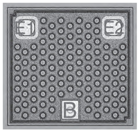
Nexperia has achieved very low saturation voltage in its range of low VCEsat BJTs by designing the emitter region of these devices to be spread across a larger die area. The layout of the base contact has a geometry which enables an even and efficient current drive for the whole active area. Low VCEsat transistors are designed to have a ‘mesh’ structure (Figure 1), in which a transistor is distributed across many corresponding cells. Apart from considerably reducing VCEsat, this also provides a constant level of high current gain (hFE). Table 1 shows how the specifications for conventional BJTs typically compare to those in low VCEsat devices.

A tradeoff associated with reducing VCEsat relates to the breakdown voltage of the transistor. Specifications in the data sheet target the VCEsat/RCEsat performance of the device and provide more detail about this relationship. Low-VCEsat transistors are available in a wide range of packages including standard (SMD SOT23, SOT89 or SOT223) as well as DFN and more power-oriented packages like LFPAK56.

Applications for low VCEsat BJTs
The load-switch
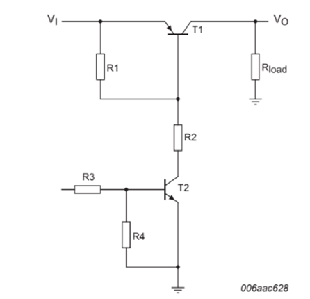
A typical application where a low VCEsat BJT can outperform a MOSFET is the load switch (Figure 2). A common version uses a combination of a high-side switch (T1) and a control transistor (T2). Here the load is ground-connected and the positive supply voltage is turned on and off. Reverse currents from the output to the input are blocked by the inherent feature of BJTs, an important feature if a load switch is used in a charger application where a battery connected to the output must not feedback current into input power supply when it is switched off. If the load transistor is realized using a p-channel MOSFET (instead of a BJT), the body diode will conduct a reverse current, so to prevent this from happening, an extra diode or a second FET is required, but this adds extra cost. Because the forward voltage of the diode must be added to the RDSon losses of the FET, the efficiency of this type of load switch is reduced. Another advantage of using a BJT is that it only requires a small control voltage, because the forward voltage of the base-emitter diode is approximately 0.7 V (a value that does not vary by much) whereas the gate-source threshold of a MOSFET can have a wider spread of values so a bigger control voltage is required. This means that if small voltages are to be switched, then a p-channel MOSFET cannot be used in the load path. A further advantage of using a low VCEsat BJT in this application is its superior ESD robustness.

DC-DC converter
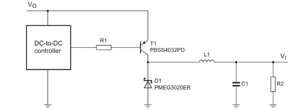
The DC-to-DC converter is another application for low VCEsat transistors which have been optimized for high-speed switching. The high and constant current gain, low saturation voltage and good switching performance of the PBSS4032PD BJT allow it to be used instead of a P-channel MOSFET.

Low-voltage dropout regulator
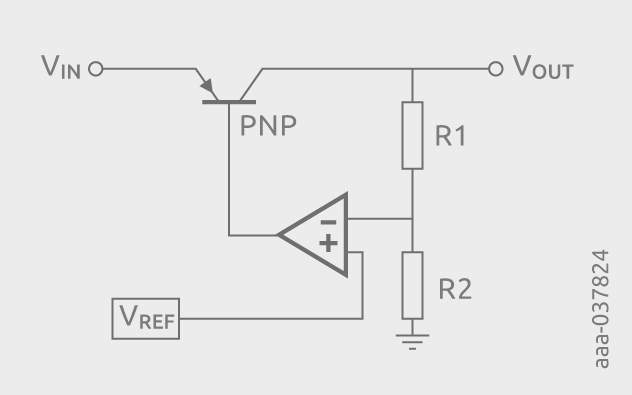
Within the family of linear regulators exists a subgroup called low-voltage dropout regulators (LDOs). While standard linear regulators require headroom between their input and output voltage of VCEsat + VBE, the headroom required by an LDO is VCEsat only. Using a low VCEsat BJT lowers this headroom even further. Figure 4(a) shows an LDO using an NPN BJT in the load path, while Figure 4(b) uses a PNP BJT. These types of linear regulators are optimal for battery-powered applications because they are highly efficient. The high forward gain of low VCEsat BJTs further increases efficiency, because lower driving currents can be used.

.2024-06-27-17-40-32.png)
Figure 4 LDOs using (a) NPN-BJT (a) and (b) PNP-BJT
Summary
Combining exceptionally low saturation voltage and high current gain, Nexperia’s low VCEsat BJTs can help to improve the energy efficiency of many power supply applications. Due to their superior performance, low VCEsat transistors can replace standard transistors in larger packages, enabling more compact designs on smaller PCBs.
To learn more about Nexperia’s low VCEsat BJTs, visit:
To learn more about Nexperia’s exclusive BJT portfolio, download our free application handbook: